Author

018. A History of Graphics Cards: Creative Hacks on MDA/CGA tags: – Graphics Card History – MDA – CGA – Text Mode – Graphics Programming – Retro Computing

dean
018. A Brief History of Graphics Cards — Part Two According to the plan, this section was supposed to cover VESA, but I felt MDA/CGA still had a lot of interesting ground to cover, so I decided to walk through some of the fun tricks people pulled off under MDA/CGA modes with everyone. The previous... » read more

017. A History of Graphics Cards: From Text Mode to the Color Palette tags: – Graphics Card History – Computer Hardware – Display Technology – MDA – CGA

dean
017. A Look Back at the History of Graphics Cards — Part 1 Recently I studied the history of graphics cards, following the x86 thread as the backbone. Here is a rough summary. The evolution of graphics cards can be divided into the following stages, which are also the major display modes: Text mode Color... » read more

016. 8th-Generation x86 Microarchitecture: Intel Core tags: – x86 – Microarchitecture – Intel – Processor Design – Computer Architecture

dean
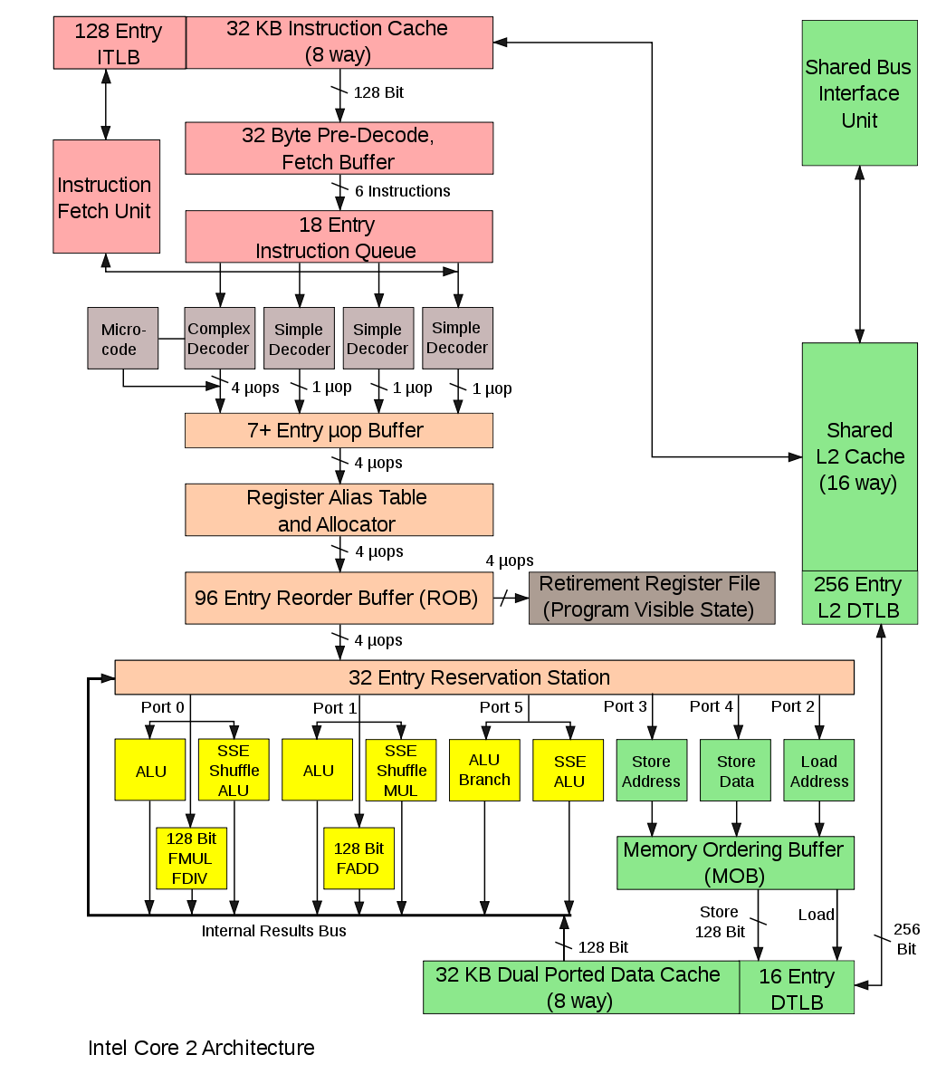
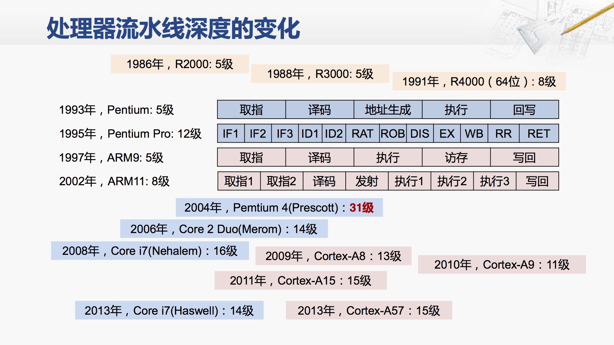
8th-Generation x86 Microarchitecture: Intel Core The Core microarchitecture is a processor internal architecture designed from scratch, but it has a design similar to Pentium M. It has a 14-stage pipeline(Pipeline), which is more than half shorter than the 31-stage Prescott of the NetBurst architecture. In addition, its execution core also increased from the 3 instructions... » read more

015. 7th-Generation x86: The Pentium 4 and Intel NetBurst Architecture tags: – x86 Processors – Intel Architecture – Computer History – Processor Technology – Hardware Design

dean
7th-Generation x86 Processor: Pentium 4 The Pentium II and Pentium III that followed the Pentium Pro were both based on the P6 architecture. They introduced no major functional or architectural improvements; instead, the fabrication process continued to advance and clock frequencies continued to rise, with the Pentium III eventually reaching a maximum of 1.4 GHz.... » read more

014. The 80686 (Pentium Pro): Architecture and Innovations tags: – CPU Architecture – SMP – Cache Technology – Instruction-Level Parallelism – Computer History

dean
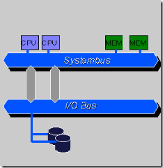
80686-Pentium Pro SMP Symmetric Multiprocessing The Pentium Pro introduced support for SMP, allowing multiple CPUs to be used in a single machine. There are two primary ways to implement a multiprocessor system. One is called SMP, or symmetric multiprocessing, and the other is NUMA, or Non-Uniform Memory Access. In an SMP system, multiple CPUs have... » read more

013. The 80586 (Pentium) Processor and Superscalar Execution tags: – CPU Architecture – Intel Processors – Superscalar Technology – x86 Microprocessors – Computing History

dean
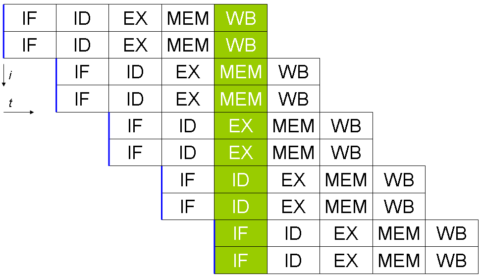
80586—Superscalar Execution in the First-Generation Pentium The first-generation Pentium was a fifth-generation microprocessor based on the macro-core x86 architecture, and it began shipping on March 22, 1993. It was the successor to the 486 product line. Pentium was originally supposed to be named 80586 or i586, but was later named “Pentium” (i586 is generally considered... » read more

012. The 80486 Microprocessor: Architecture and Features tags: – CPU Architecture – x86 Processor – Computer History – Microprocessor Technology – Hardware Design

dean
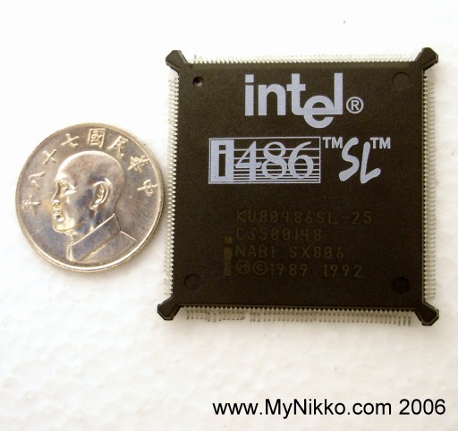
Slight Improvements to the 80486 The 80286 added segmented memory management and protected mode. The 80386 added paged memory management. These both had an enormous influence on modern operating systems. Because after the improvements in the 386, no more changes of such magnitude took place — the 80386 became a timeless classic. So much so... » read more

010. Paged Memory Management in the 80386

dean
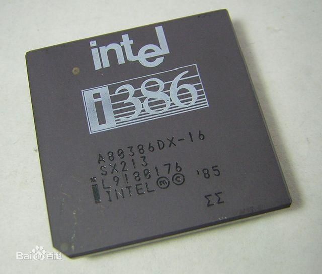
Paged Memory Management in the 80386 INTEL introduced the 80386 chip in 1985. It was the first 32-bit microprocessor in the 80×86 series, and its manufacturing process was also a major advance. Compared with the 80286, the 80386 contained 275,000 transistors. Its clock frequency was initially 12.5 MHz and was later increased to 20 MHz,... » read more

009. The Evolution of the x86 Computer Architecture” tags: [“x86”, “architecture evolution”, “processor”, “compatibility”]

dean
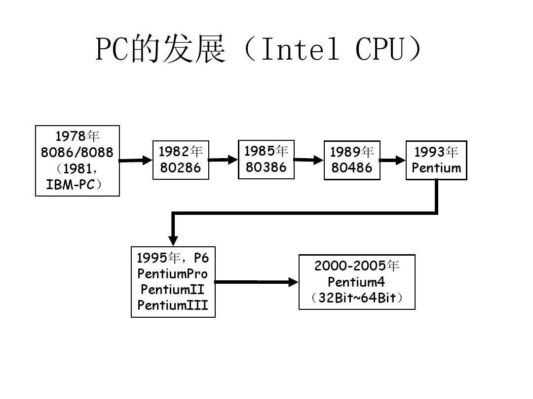
The Evolution of the x86 Computer Architecture We know the first x86 chip was the 8086, followed by the 80286, 80386, 80486, Pentium… This article uses many images to walk everyone through the development history of x86 computers, so you can understand when each part of today’s computers was added, and what historical event each... » read more

008. 8086 Interrupt Handling

dean
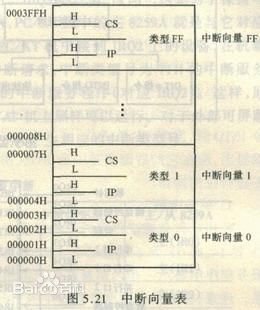
8086 Interrupt Handling Interrupt Vector Table The 8086 supports 256 interrupts, each requiring a corresponding Interrupt Service Routine (ISR). The starting addresses (CS:IP) of the 256 ISRs are arranged in order to form an Interrupt Vector Table (IVT). Each interrupt vector consists of 4 bytes. These 4 bytes specify the segment value (assigned to CS)... » read more

007. The 80286 Task State Segment and Task Switching

dean
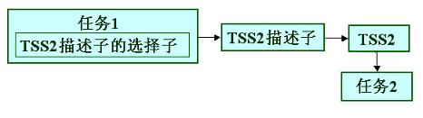
The 80286 Task State Segment and Task Switching Call gate descriptors are used for system calls Interrupt gate descriptors are essentially a new interrupt vector table Task state descriptors are used to save task state during task switching Tasks An example of a task is a process. An example of task switching is process switching.... » read more

006. The 80286 Call Gate Descriptor

dean
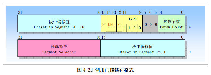
The 80286 Call Gate Descriptor In addition to segment descriptors used to restrict memory access, the 80286 also has gate descriptors used to restrict transfers of program control. The 80286 has four kinds of gate descriptors: call gate descriptors, interrupt gate descriptors, trap gate descriptors, and task gate descriptors. These descriptors are also stored in... » read more

005. A Detailed Look at the 80286

dean
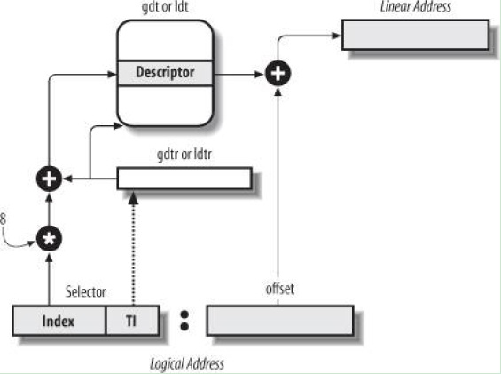
Overview An x86 CPU operates in real mode, protected mode, virtual 8086 mode, system management mode, and so on. An x86 CPU can only enter real mode at startup. Once it has switched to protected mode, it can never return to real mode. Real Mode and Protected Mode Put simply, real mode is the mode... » read more

004. CPU Cache Architecture

dean
Bridging the Gap The purpose of cache is to bridge the speed gap between memory and the CPU. CPU instructions execute in less than a nanosecond, while memory-access latency ranges from a dozen to several dozen nanoseconds. For a single memory access, the CPU must therefore wait for dozens or even hundreds of clock cycles,... » read more

003. Wear Leveling in NAND Flash (wear-leveling)

dean
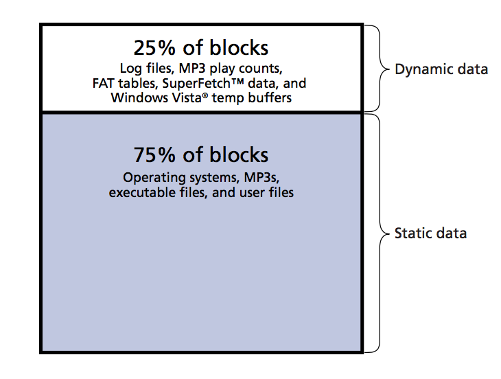
1. The Importance of Wear Leveling The purpose of wear leveling is to prevent some blocks from going bad too early, thereby reducing reliability. It tries to distribute erase operations as evenly as possible across different blocks so that they all reach the end of their lifespan at roughly the same time. Flash storage is... » read more

002. NAND Flash Fundamentals

dean
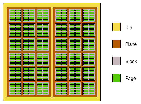
1. Packaging In a NAND flash chip, a single silicon wafer packaged inside is called a Die. A Die may internally be divided into two planes, each called a Plane. A Plane contains multiple Blocks, and each Block is further divided into multiple Pages. Usually people do not concern themselves with the Die and Plane,... » read more

001. The x86 Boot Process

dean
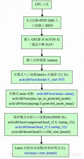
1.1 The CPU’s First Instruction Borrowing an image from a friend online, it walks through the flow from x86 system boot all the way to the Linux kernel. From the diagram we can see that after power-on, the CPU fetches and executes its first instruction from address CS:IP = FFFF:0000. This instruction belongs to the... » read more